Proposals for the Current industrial development
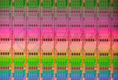
With the continuous development of laser technology and the penetration of laser technology into the semiconductor industry, lasers have obtained very good application effects in multiple production processes in the semiconductor field. With laser marking, precise marking of semiconductor chips is no longer a difficult problem. Laser cutting semiconductor wafers, laser cutting semiconductor wafers, and the defects of traditional contact blade cutting have been modified to solve the problems of easy chipping of the blade, low cutting efficiency, and easy damage to the surface structure. Under the requirements of increasingly smaller integrated circuit process line widths, LOW-K materials (K is a dielectric constant, that is, low-permittivity materials) are increasingly used for integrated ICs. In view of the fact that the LOW-K layer is difficult to process with the traditional process, a laser grooving process is introduced, and the LOW-K layer is removed from the cutting path by laser. At present, 12-inch silicon wafers are widely used in the field of semiconductor integrated circuits. As the wafers become thinner and thinner, the thin wafer is bonded to the carrier wafer and then the two parts are separated by debonding and laser demolition The key has become a hot spot for its many advantages such as high efficiency and no consumables. In addition, laser has achieved good application results in drilling, scribing, annealing and other processes.
Guoyu Technology’s laser automation equipment is very diversified. It has provided different types of laser equipment used in semiconductor manufacturing processes, including MiniLED cutting, wafer sorting, chip inspection, and patterned flexible circuit boards, IC substrates and semiconductor device processing applications.
industrial proposal with laser application
-
The grinding wheel blades from Japanese Disco company are still using in the majority of the existing mass-produced cutting and processing, but as the chip size becomes smaller and the processing accuracy becomes more and more precise, the non-contact processing method offered by laser is becoming outstanding for its advantages. In recent years, with the development of the mini Led market, a cutting device is urgently needed to solve the mass production problem. The high-precision cutting system developed NBI meets the needs of the market. The cutting line width is controlled below 30μm, and the spot diameter can be below 10μm; fully meet the production needs of the industry
-
After the wafer is cut, the wafer will be cleaned, tested and sorted. NBI integrated the testing and sorting into one machine so that the aberrations and errors that occurs when switching to a new working station will be minimized (but this methods can only be applied on the products with the same tempo. Therefore, NBI will offer separated testing and sorting device as well. To remove the non-qualified and waste material from the well-cut and processed wafer, testing and sorting device will be needed. The accuracy can be precise down to every pixel within 0.5μm range.
-
With the emergence of micro-bump wafers, measurement and inspection is face huge challenges. The most basic requirement for it is that any feasible inspection must be able to achieve the required resolution and sensitivity to measure the feature of micro-bumps. The chip for making 25μm bumps on a 50μm pitch is currently under development, and technologies for smaller bump diameters and pitches are also under development. In addition, when the number of bumps on a single chip exceeds 10,000, the wafer inspection system must be able to handle the rapid increasing number of bumps and wafers. Analysis software and computer hardware must have high enough performance to store and process the coordinate and topographic data of millions of bumps on each wafer.
1. In laser trigonal measurement, a finely focused laser beam is used to scan the surface of the wafer, and the optical system focuses the reflected laser onto the detector. When using 3D laser trigonal measurement to detect the topography of micro bumps, its advantages are shown in terms of accuracy, speed, and detectability.
- 2. Particle test
- Particle control is an important link in the wafer processing and device manufacturing process. Particle monitoring is also very important. There are two working principles for particle testing equipment, one is the light scattering method; the other is the light extinction method.
- For particles suspended in gas, the light scattering method is usually used for testing. At the same time, some manufacturers use this working principle to produce equipment for testing particles on the wafer’s surface; for particles in liquid, both methods are applicable.
- 2. Particle test
-
The semiconductor wafer laser invisible cutting technology developed by NBI is a new laser cutting technology, which has many advantages such as fast cutting speed, no dust, no damage to material, less cutting difficulty, and complete dry condition, etc. The main principle of invisible cutting is to concentrate a short pulse laser beam through the surface of material’s center and form a metamorphic layer. External pressure will be applied to separate the chips.


